Quantum-Safe Networks Are No Longer Theoretical
The telecom industry is entering a phase in which quantum security is no longer a laboratory topic but an operational and strategic issue for networks, supply chains, and regulation.
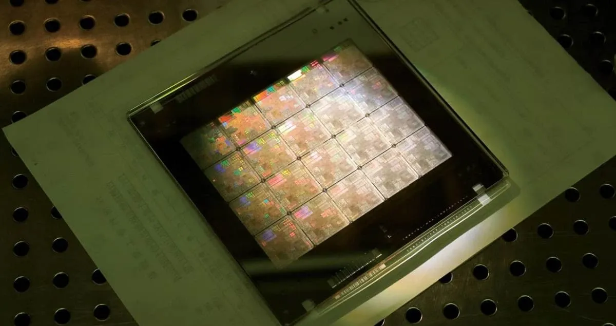
TSMC is moving to production with NVIDIA’s computational lithography platform, called cuLitho. The chipmaker expects to accelerate manufacturing and push the limits of physics for the next generation of advanced semiconductor chips.
A critical step in the manufacture of computer chips, computational lithography is involved in the transfer of circuitry onto silicon. It requires complex computation, involving electromagnetic physics, photochemistry, computational geometry, iterative optimization, and distributed computing. A typical foundry dedicates massive data centers for this computation, and yet this step has traditionally been a bottleneck in bringing new technology nodes and computer architectures to market.
Computational lithography is also the most compute-intensive workload in the entire semiconductor design and manufacturing process. It consumes tens of billions of hours per year on CPUs in leading-edge foundries. A typical mask set for a chip can take 30 million or more hours of CPU computing time, necessitating large data centers within semiconductor foundries. With accelerated computing, 350 NVIDIA H100 Tensor Core GPU-based systems can now replace 40,000 CPU systems, accelerating production time, while reducing costs, space, and power.
NVIDIA has also developed algorithms to apply GenAI to enhance the value of the cuLitho platform. A new GenAI workflow has so far delivered an additional 2x speedup on top of the accelerated processes enabled through cuLitho. This enormous speedup of computational lithography accelerates the creation of every single mask in the fab, which speeds up the total cycle time for developing a new technology node. More importantly, it makes possible new calculations that were previously impractical.

The telecom industry is entering a phase in which quantum security is no longer a laboratory topic but an operational and strategic issue for networks, supply chains, and regulation.

Huawei sees the next stage of consumer-device competition in Europe at the intersection of openness, health functions, local data processing, and new hardware form factors.

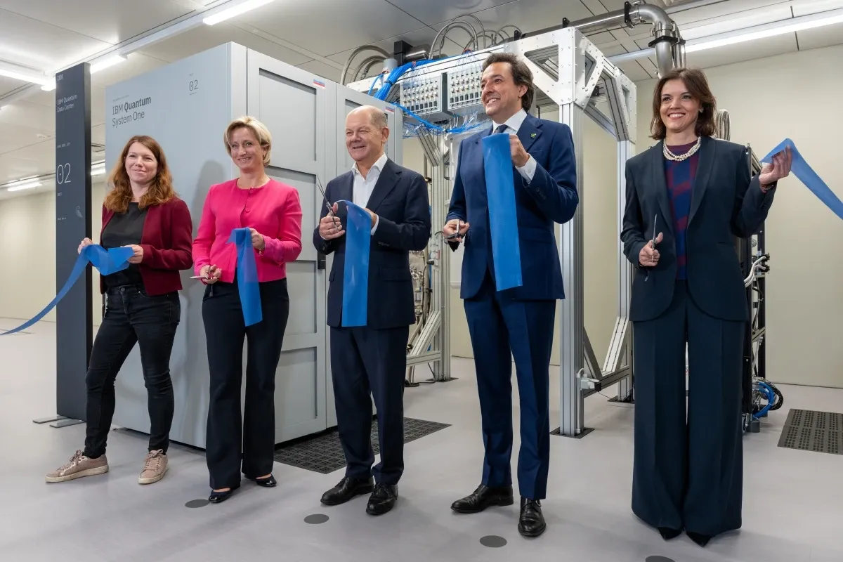
IBM unveiled the industry’s first published quantum‑centric supercomputing reference architecture.